Black Pad Defect
When a BGA component fails most people think it is due to a defective component or improper assembly. This is usually not the case. There are many variables that affect BGA components that will not normally affect other components on the circuit board. Before we start assembly there are items that we can check to assure success.
What is Black Pad?
One of the most common problems that result in mysterious opens on BGA components is “Black Pad”. “Black Pad” primarily affects BGA components and will occur when using electroless nickel/immersion gold finishes on the circuit board fab. It is not visually evident on the bare fab and is usually detected after the failed BGA has been removed.
The cause of this is due is a layer of oxidation that prevents electrical connection to the circuit board. When an ENIG surface finished PWB undergoes soldering, the solder must adhere to the underlying electroless nickel plate. This is because the immersion gold is so thin that all of the gold dissolves into the solder upon soldering. The solder bonds directly to the electroless nickel.
If that nickel surface is contaminated in some way, the resulting joint will be weak and the location of failure will be directly below the surface of the nickel by leaving both nickel and phosphorous (a normal constituent of electroless nickel) on both the pad and the failed solder joint surface.
"Black Pad" is a defect related to ENIG boards. It is a separation of solder joints formed to the surface of the electroless nickel underplate. This is commonly attributed to excessive phosphorous in the electroless nickel (i.e. nickel electroless bath out of control). However, any kind of nickel contamination (phosphorous or not) that results in the failures characterized here, are often reported as "black pad" failures.
In short, “Black Pad” is caused by too much phosphorus, and or contamination in the nickel plating bath. It is not visually detected prior to assembly because gold is plated over the nickel.
Black Pad Indications
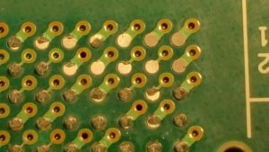
Indications of “Black Pad” Once you have assembled your BGA to the board. The X-ray image looks excellent with uniform balls, no bridging, and minimal voids. You have done a visual inspection of the perimeter BGA balls at 20X and observed uniform ball compression and good wetting. Everything looks good, but the BGA tests with an electrical open, intermittent opens, and or will work if you exert pressure on the chip. This is s sign of possible black pad. If it were cold solder, or insufficient reflow. That would most likely be evidenced during the visual perimeter inspection. At this point you may remove the suspect component and inspect the surface finish on the circuit board and on the BGA. “Black Pad” will appear as a dull grainy black or grey color pad with evidence of non-wetting or de-wetting.
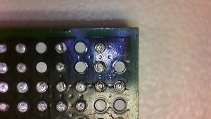
Below are illustrations of what the Black Pad defect will look like. Don't mistake Black Pad for Lead Free Oxidation. Lead Free Oxidation looks like a Silver/Grey color. Black Pad looks like a burned black/brown color.
For best yields with Lead Free Solder use an active flux. If you must use No-Clean Flux, then a Nitrogen or Vapor Phase Reflow Oven is best.
Non-wetting at PCB caused by Black Pad

Non wetting at BGA caused by Oxidation.

Ready to find out more?
Contact Us Today