How to Fix a Missing Solder Pad
How to Fix a Missing Solder Pad
Printed circuit boards are the backbone of electronic devices, facilitating the connection and flow of electrical signals between components. PCBs play a fundamental role in diverse industries, from consumer electronics to aerospace applications. As electronic devices become more intricate, soldered connections must offer as much reliability as possible.
Solder pads attach electronic components to ensure proper electrical conductivity. Maintaining PCB pads' integrity is vital to ensure electronic devices' functionality and longevity of electronic circuits.
PCBs and solder pads are susceptible to damage. You may have noticed a soldering pad came off, necessitating PCB pad repair. Here is your guide to repairing broken solder pads so you can continue using the PCB instead of discarding it.
What Are Solder Pads?

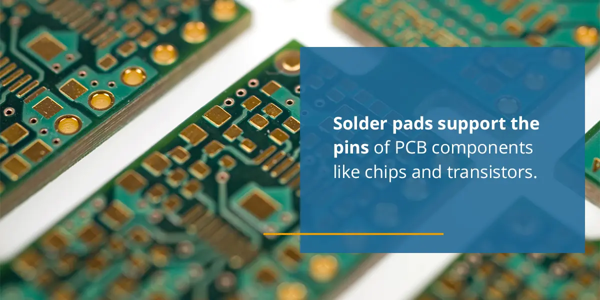
Solder pads support the pins of PCB components like chips and transistors. These small areas — typically made of copper for high conductivity — allow you to attach electronic components and are crucial junctions that ensure the smooth transmission of signals across the PCB.
Missing or damaged solder pads prevent the PCB from operating effectively, so fixing and cleaning them is essential for maintaining electrical continuity, minimizing signal loss and ensuring the device's reliability.
How to Fix Broken Solder Pads — Materials and Steps
You must follow a specific process to repair a lifted soldering pad. Fixing solder pads lets you keep using your circuit boards instead of discarding them. You'll need these materials to prepare for your solder pad repair.
- Isopropyl alcohol and wipes
- Lint-free cloth or compressed air
- Microscope or magnifying glass
- C-clamps
- Solder and soldering iron
- Circuit frame
- Flux
- ESD-safe Kapton tape
- Safe ESD cutting surface
- Epoxy resin and hardener
- Toothpicks
- X-Acto knife
Though every PCB pad repair will vary, fixing broken or missing solder pads typically includes these 10 steps. Once you have your supplies, you can begin cleaning and repairing a solder pad.
- Clean the existing solder pad: To begin, use isopropyl alcohol to thoroughly clean the solder pad area and remove any remaining grime, dirt or other debris. After cleaning the damaged pad, dry the spot with compressed air or a lint-free cloth.
- Remove the pad: Next, carefully cut away any remaining traces of the pad with an X-Acto knife. Using a sharp knife is best, as it allows you to be precise and reduces the risk of causing more damage to the circuit track. You should also remove a short section of the connecting circuit.
- Clean under and around the pad: Once you have removed the pad, use isopropyl alcohol to clean the areas around and under where it sat. If there is burned or damaged laminate in this area, remove it thoroughly during this step.
- Remove the remaining solder mask: Use a toothpick to remove any remaining solder mask from the connecting circuit or conductor.
- Clean the area again: Thoroughly clean and prep the area with more isopropyl alcohol. Dry the PCB with compressed air or a lint-free cloth.
- Tin the conductor: The appropriate solder alloy will vary depending on the PCB and conductor — once you have the correct alloy, tin the conductor. You can also apply flux to the exposed connecting circuit at this stage.
- Select circuit frame: Use an X-Acto knife to cut out and trim a new conductor from a corresponding circuit frame. The length should allow maximum circuit overlap to make soldering clean and easy.
- Tin the new pad: First, tin the pad where it overlaps the exposed circuit with the solder alloy. Next, mix the epoxy resin with the hardener and put a small amount where you will place the new pad on the PCB. You can cure the resin in the open air or an oven, as long as you follow every manufacturer's guideline.
- Solder the pad and conductor: Use high-temperature-rated Kapton tape to align and secure the new pad in place. Make a lap joint with a small amount of the solder alloy to ensure a reliable connection.
- Clamp and cure: Clamp the new pad in place, coat the solder joints in the epoxy mixture and cure them properly. After curing, remove the clamp and use isopropyl alcohol to clean the pad a final time. Now is your chance to test the new solder pad's electrical continuity. Once you're sure the solder pad and circuit work properly, you can apply the epoxy mixture around the new pad's edges to increase the mechanical strength of the entire area.
How to Clean a Solder Pad
Here are a few safe and reliable methods for cleaning PCB solder pads.
- Milling machines: Milling machines are incredibly sharp, making this method precise and effective. However, skill and machine experience are necessary to carefully control the blade depth — otherwise, you could penetrate the board. You may need a microscope to provide a sharp view of the work and get adequate visuals.
- Scraping and grinding: Grinding and scraping the solder pad is one of the most common ways to clean it. A trained technician commonly uses a knife or scraper to remove layers of the solder pad. This manual process can be tiring, though mechanical erasers can speed up the work. You may want to combine scraping with other methods, especially for large, extensive projects.
- Micro-blasting: This technique is most useful when cleaning solder pads from several sections of a single circuit board. The operator blasts abrasive metal through a handheld, pencil-shaped tool for accuracy.
- Chemical stripping: Chemical stripping is one of the most effective methods for cleaning solder pads. To secure the other circuit board areas, apply protective materials before using a brush or swab to apply the stripping chemical. The chemical will quickly clean the solder pad, though caution is crucial to prevent other PCB components from deteriorating.
Safety precautions are vital, whether working with a small PCB or cleaning a large board. Protect yourself and your work area from chemicals or flying debris — limiting the risk of injuries while cleaning solder pads should be a priority.
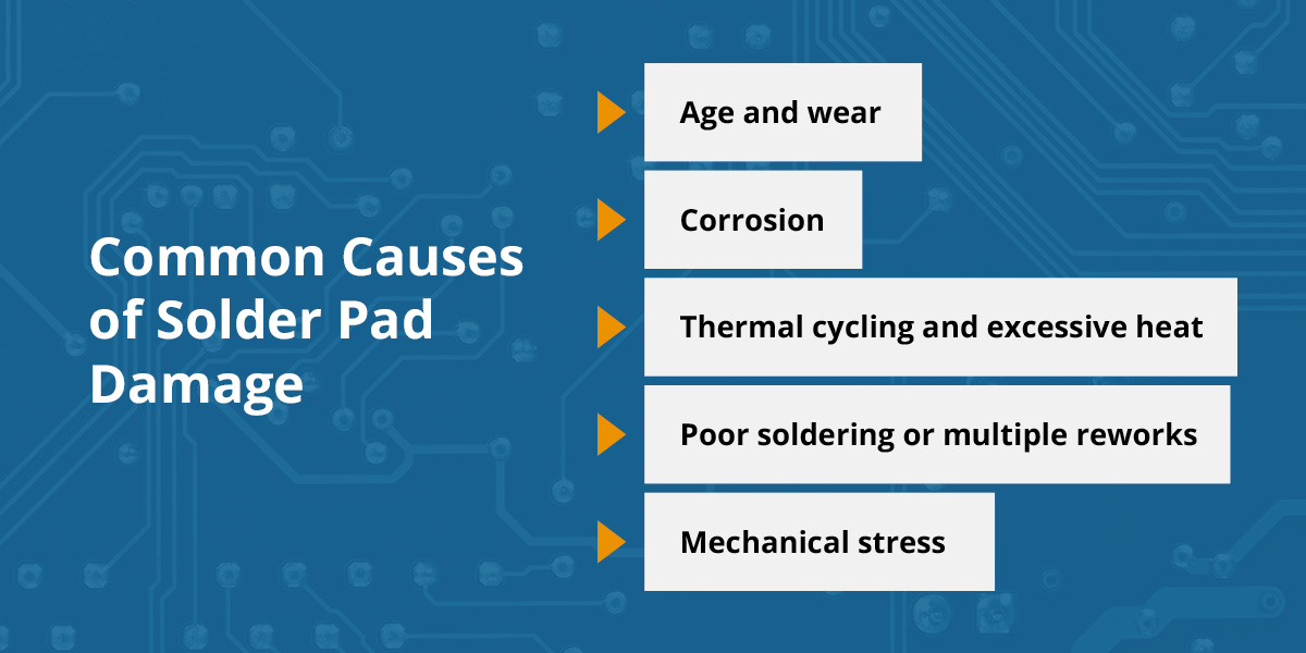
Common Causes of Solder Pad Damage
In addition to mastering PCB pad repair, understanding the potential causes of solder pad damage is imperative for engineers, technicians and others tasked with risk mitigation and electronic device repairs and maintenance. You can ensure PCB longevity and reliability by promptly identifying and addressing the issues. Furthermore, you can proactively implement measures to reduce or eliminate such risks.
Though this list is not exhaustive, here are common causes that lead to damage and the need for PCB pad repair.
- Age and wear: Over time, electronic devices will likely experience wear and tear that degrades solder pads, which could lead to cracks, the soldering pad coming off or other structural issues that would lead to impaired electrical connectivity. Periodic maintenance is crucial to prevent aging-related issues.
- Corrosion: This factor is less about the quality of the board and soldering and more related to the housing or casing and environmental factors. Exposing PCBs to moisture, chemicals or other pollutants will lead to oxidization over time, undermining the boards and pads.
- Thermal cycling and excessive heat: These issues can be due to soldering and desoldering, environmental changes or temperature fluctuations during operation. Determine the cause, as it could lead to repeated pad lifting and delamination of the copper.
- Poor soldering or multiple reworks: Using inadequate soldering techniques during manufacturing or repairs — such as improper temperature control or insufficient solder application — can lead to weak or incomplete bonding. Similarly, multiple reworks will result in pads wearing out and could lead to a lifted soldering pad.
- Mechanical stress: Stress is sometimes unavoidable, but sometimes, you can find solutions to mitigate or reduce the mechanical strain and physical force on the electronic components. Mishandling during assembly and maintenance or vibrations, drops and knocks in operation can compromise PCB integrity.
Importance of Fixing Solder Pads
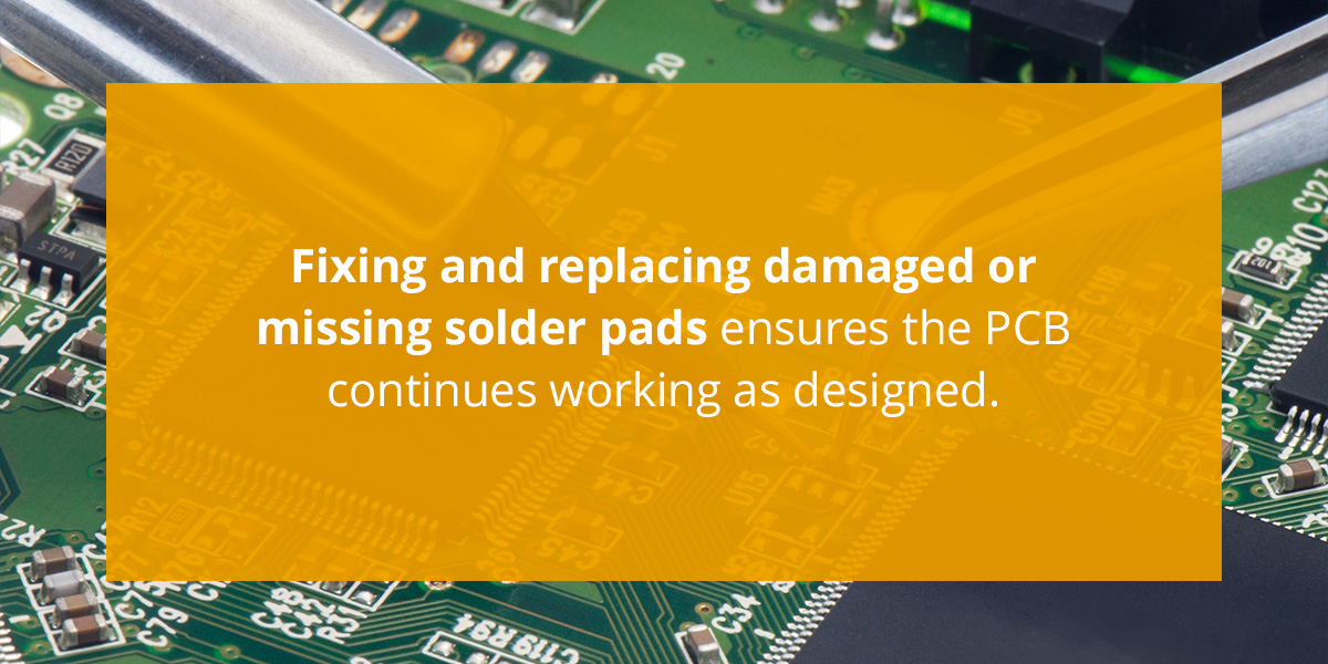
As mentioned above, fixing and replacing damaged or missing solder pads ensures the PCB continues working as designed. Without complete circuits, your devices will operate ineffectively, if at all, potentially causing more damage to the PCB and devices.
Additionally, fixing your solder pads prevents the need to keep replacing your PCBs. Discarding PCBs involves a more in-depth process than merely throwing them in the trash. PCBs contain potentially hazardous materials that require recycling or proper disposal to protect the environment and prevent them from entering landfills.
Recycling PCBs requires separating the metal and non-metal components, safely discarding or reusing them for less technical applications.
Choose Precision PCB Services for Your PCB Repair Needs
If you and your team need more guidance to confidently handle PCB repairs, ask us about our all-inclusive PCB repair training, a practical two-day course based on IPC-7721 training.
With careful instruction and ongoing feedback, you'll learn the entire solder pad repair process, including components such as cutting traces from the circuit frame library and joining them to the traces on the existing PCB.
For more information on PCB repair and our extensive training services, or to learn more about our PCB and BGA services, please contact us online or call us at 888-406-2830 today!

